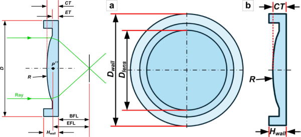
Practical large-field-of-view (FOV), high-resolution imaging of microfeatures is demonstrated through the geometry-optimized design, precision fabrication, and actual application of reattachable optical lenses and deep learning super-resolution with residual and attention mechanisms. The presented approach to the elastomeric reattachable lens addresses key limitations of metal-based lenses and metalenses, including high manufacturing cost and complexity and material constraints. Ray-tracing simulations are performed to optimize lens curvature and geometry, minimizing aberrations and improving effective focal performance. The polydimethylsiloxane (PDMS) lens, with less than 2% deviation from the designed geometry, is fabricated by the high-precision mold-assisted soft-contact printing with its effective focal length and modulation transfer function closely matched to the simulation results. This geometry-optimized PDMS lens, when conformally attached to a commercial camera module, significantly improves spatial resolution, enabling visualization of fine microstructures without altering or realigning the host system. The deep learning super-resolution model is configured to capture inter-channel features using residual and attention algorithms, and to accurately separate and restore distorted objects during the reconstruction of low-resolution images to high-resolution output. This computational-optical synergy provides wide-field, low-magnification images with high-magnification reconstructions with enhanced clarity and detail while maintaining their large FOVs. This work underscores how data-driven informatics and precision optical engineering can be seamlessly integrated to establish a scalable and versatile high-quality imaging platform without expensive components and tedious procedure. The proposed framework showcases strong potential for such as semiconductor inspection, portable diagnostics, and security and surveillance where precise microfeature analysis at high speed and low cost is required.
